1. 준비하기
1.1 필수 준비 요소
CameraLink 프로토콜을 지원하는 Frame Grabber가 필요합니다.
Frame Grabber가 하기 사양을 충족하지 못하는 경우 연결이 안될 수 있습니다.
GenICam(GenApi) : Ver_2.3.1 SFNC : Ver_2.0.0 GenICam_CLProtocol_Standard : Ver_1.1 1.2 SDK
크래비스 CameraLink 카메라는 크래비스에서 제공하는 SDK를 이용하여 카메라 연결 및 카메라 환경 설정이 가능합니다.
크래비스 SDK 다운로드 링크 : CamGuideCL.zip
1.3 주의사항
동작 온도 : 0℃ ~ +45℃ 누수 및 습기 주의 자기장 및 전기장 환기 초기 동작 상태 제품 성능은 Cable 특성에 따라 달라질 수 있습니다.
CE 규격 준수를 위해 표준 Camera Link™ Cable 또는 동급 이상의 Shield 특성이 좋은 케이블을 사용해야 합니다. (추천 Cable : 3M 14B26-SZLB-xxx-SKC)
제품의 기능 및 성능 개선을 위해 예고 없이 수정될 수 있습니다.
2. 제품 사양
2.1 제품 개요
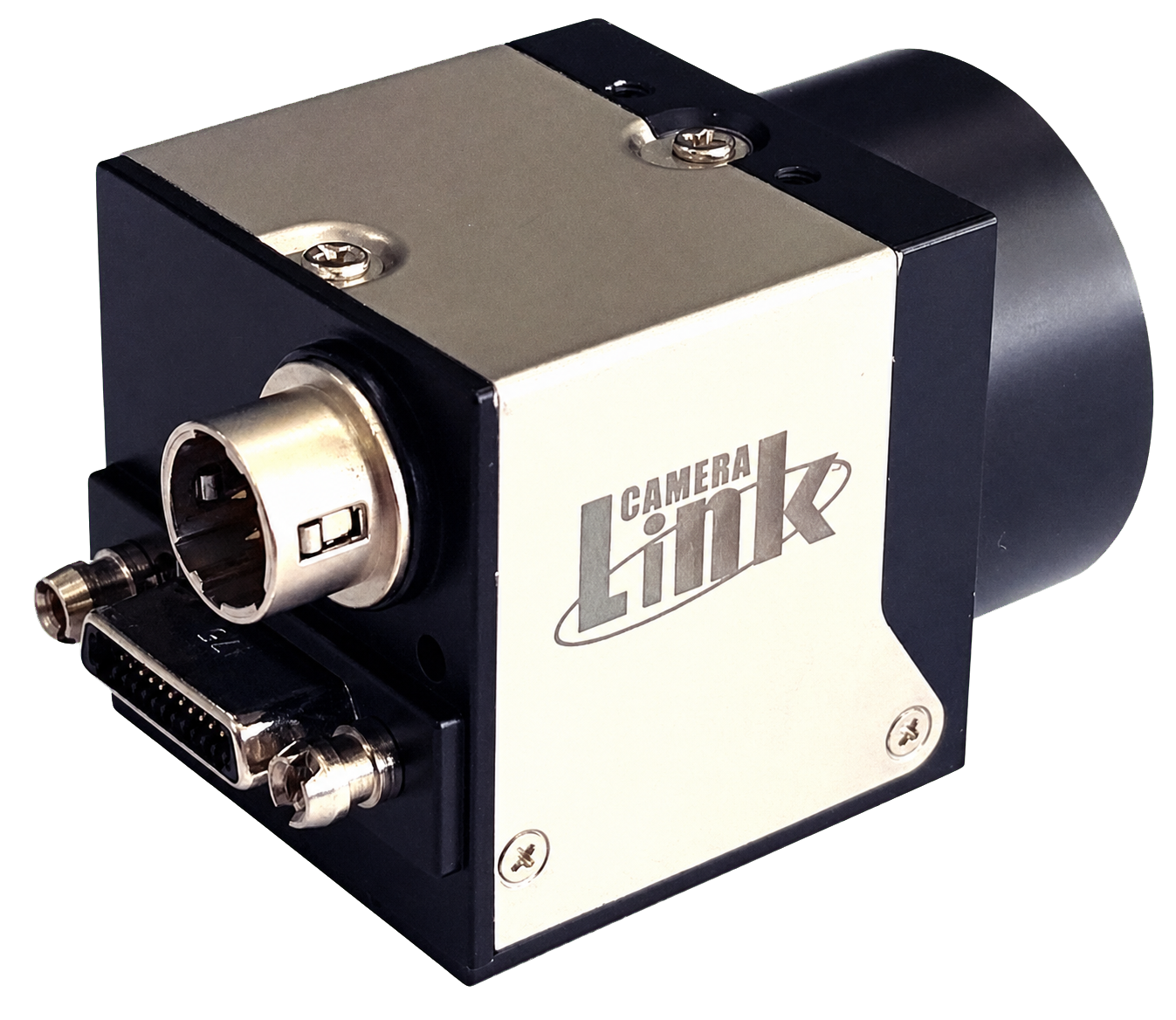
Sony CMOS Sensor Camera ROI Scan 지원 Freerun 및 Trigger Mode 지원
CameraLink Interface External General Purpose I/O(TTL) 2ch 지원
Power supply : DC 24V (10.8 ~ 26.4V range supported)
2.2 주요 사양
Spec. MC-A040M/K-523 MC-A160M/K-154 MC-A320M/K-55 MC-A500M/K-35 MC-A121M/K-20 MC-A121R/L-20
Sensor 0.4M 1.6M 3.2M 5M 12.2M 12.1M Sensor Size 1/2.9″ 1/2.9″ 1/1.8″ 2/3″ 1.1″ 1/1.7″ Pixel Size (µm) 6.90 × 6.90 3.45 × 3.45 3.45 × 3.45 3.45 × 3.45 3.45 × 3.45 1.85 × 1.85 Resolution (3Tap) 720 × 540 1440 × 1080 2048 × 1536 2448 × 2048 4096 × 3000 4016 × 3036 C/L Pixel Freq. 85MHz 85MHz 85MHz 85MHz (60MHz) 85MHz 85MHz C/L Tap 3Tap / 2Tap / 1Tap Frame Rate (Max)* 523.5fps 154.6fps 55.7fps 35.7fps (35.0fps) 20.3fps 20.0fps Scanning Method Full / ROI / Reverse (X,Y,ALL) Full / ROI / Reverse Full / ROI / Reverse Full / ROI / Reverse Full / ROI / Reverse Full / ROI / Reverse (X,Y,ALL) Synchronization Internal(Freerun), External(CC1~4 or Circular), Software trigger via PC Trigger Mode Timed, Trigger Width GPIO Transistor-Transistor-Logic(TTL) Input/Output 2ch Shutter Global Shutter Rolling Shutter / Global Reset Shutter Speed 1µs ~ 3sec 1µs ~ 3sec 1µs ~ 3sec 1µs ~ 3sec 1µs ~ 3sec 213.13µs ~ 3sec Gain Abs Analog : 0dB ~ 24dB (1× ~ 15.8×) Analog : 0dB ~ 28dB ADC Bit Depth 8/10/12bit 8/10/12bit 12bit 12bit 12bit 10bit Black Level (Analog) 0~255(8bit) 0~255(8bit) 0~4095 0~4095 0~4095 0~255 Black Level (Digital) 0 ~ 1023 (10bit) Gamma Gamma Correction (0 ~ 3.999) / Adjustable LUT (10bit to 10bit) Interface Mini CameraLink / PoCL Mini CameraLink (SDR) Communication RS232 via CameraLink connector Pixel Data Format Mono Model : Mono8/10 SNR B/W 37dB B/W 31dB B/W 36dB B/W 37dB B/W 39dB B/W 38dB Function Control BalanceWhiteAuto < Off / Once / Continuous (Only Color Models) > Lens Mount C mount Optical Accuracy Optical center ≤ ± 0.2 mm Power Requirements DC(12V ~ 24V ± 10%) or PoCL Consumption < 1.9W < 2.0W < 1.9W < 1.9W < 2.2W < 1.7W Weight 44g Dimensions 29 × 29 × 29㎜ (Without mount, Connector) Temperature Operating : 0℃ ~ +45℃ (with < 20~80% RH) / Storage : -20℃ ~ +60℃ Vibration / Shock 98m/s² (10.0G) / 196m/s² (20.0G) Standard Compliancy CE (EN61326-1; 2006년; Class A) Conformity RoHS / WEEE
3. 카메라 인터페이스
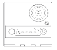
3.1 Back Panel
No. Name Remark 1 CameraLink Connector SDR26 2 Power & External I/O Connector 6Pin Circular 3 LED Indicator LED
3.2 카메라 DC IN / External I/O Pin Map
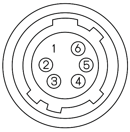
1) 6 pin Circular Connector
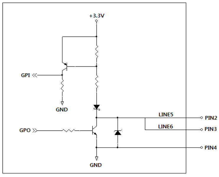
No. Name IN/OUT Description Remark 1 DC VCC IN 10.8 ~ 26.4V Input Range 2 GPIO1 IN/OUT TTL / Input : 3.3V ~ 24V / Out : 3.3V Line 5 3 GPIO2 IN/OUT TTL / Input : 3.3V ~ 24V / Out : 3.3V Line 6 4 GPIO GND IN 5 NC - 6 DC GND IN
3.3 CameraLink Connector Pin Map
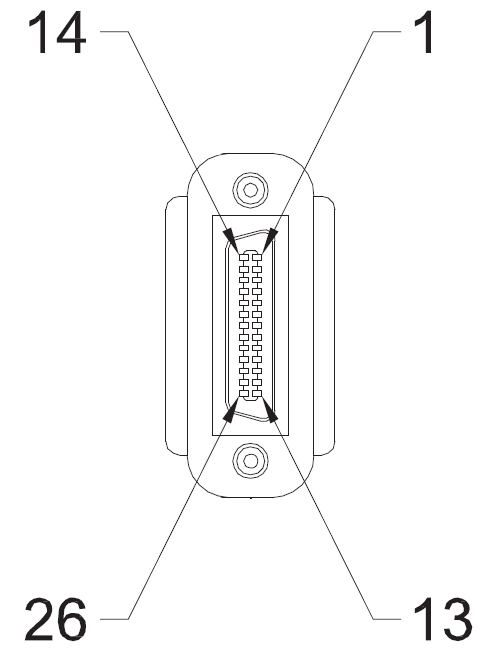
1) Mini CameraLink™ Connector (SDR)
Pin No. Signal Name Pin No. Signal Name 1 GND 14 GND 2 X0- 15 X0+ 3 X1- 16 X1+ 4 X2- 17 X2+ 5 Xclk- 18 Xclk+ 6 X3- 19 X3+ 7 SerTC+ 20 SerTC- 8 SerTFG- 21 SerTFG+ 9 CC1- 22 CC1+ 10 CC2+ 23 CC2- 11 CC3- 24 CC3+ 12 CC4+ 25 CC4- 13 GND 26 GND
3.4 LED Status
Light Status Orange 카메라 초기화 Green 정상 동작
3.5 External I/O 내부 회로
GPIO (TTL)
3.6 CameraLink Interface Timing
3.6.1 Data Order of the CameraLink
3.6.2 Mono or Color Bayer Order
3.6.3 Color RGB Order (8bit)
4. 카메라 기능
4.1.1 Device Tap Geometry
Device Tap Geometry를 설정하는 기능입니다. 해당 Tap에 맞게 Frame Grabber camfile을 변경해야 합니다.
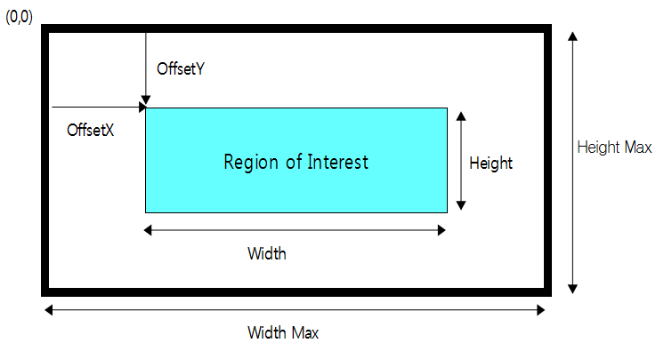
4.1.2 ROI (Region Of Interest)
WidthMAX ≥ Offset X + Width
Width, Height, Offset X, Offset Y를 설정함으로써 사용자가 원하는 영역만 받는 것이 가능합니다. 또한, 사이즈가 작아질수록 fps가 증가합니다.
ROI Setting 4.1.3 Binning Vertical
수직의 2-Pixel을 합하여 Frame Rate 속도가 2배가 되도록 설정하는 기능입니다.
4.1.4 Binning Horizontal Vertical
수평의 2-Pixel을 합하여 Frame Rate 속도가 증가하도록 설정하는 기능입니다. 단독으로 값을 조절할 수 없으며, Binning Vertical이 활성화되면 추가로 조절 가능합니다.
4.1.5 Decimation Vertical
수직으로 1-Pixel씩 건너뛰어 Frame Rate 속도가 2배가 되도록 설정하는 기능입니다.
4.1.6 Decimation Horizontal
수평으로 1-Pixel씩 건너뛰어 출력하여 Frame Rate 속도가 증가하도록 설정하는 기능입니다.
※ 모델별 Binning(Bin) 및 Decimation(Sub) 지원 현황
Image Mode MC-A040x-523 MC-A160x-154 MC-A320x-55 MC-A500x-35 MC-A121x-20 MC-A121R/L-20 Binning Vertical X O (Only Mono) X X X X Binning Horizontal Vertical X O (Only Mono) X X X X Decimation Vertical X O O O O X Decimation Horizontal X O O O O X
※ MC-A160M-154만 Binning Vertical 및 Binning Horizontal Vertical을 지원합니다.
4.1.7 Reverse X, Y
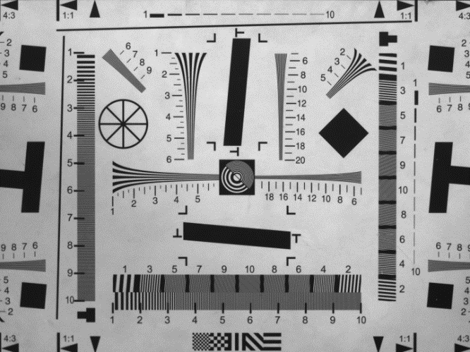
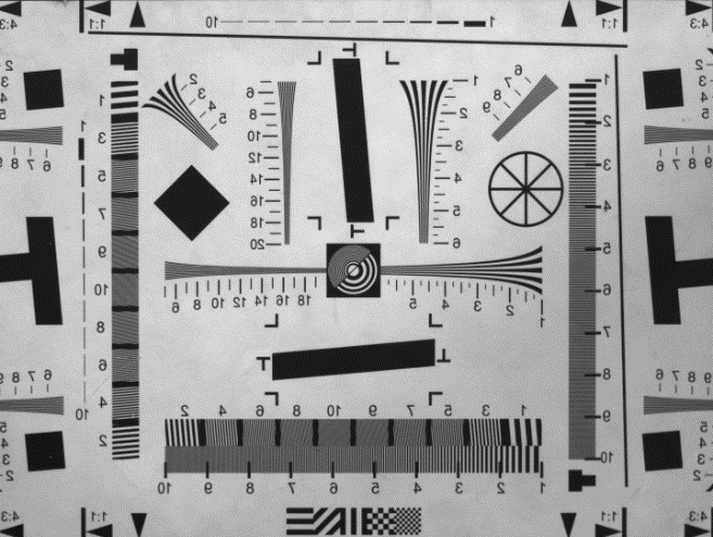
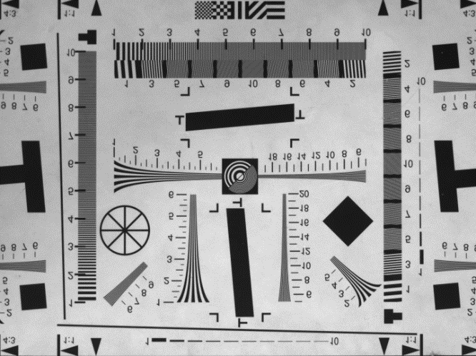
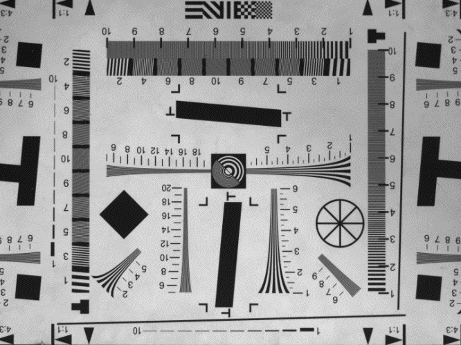
영상의 좌/우, 상/하를 변경하여 보는 기능입니다. Reverse X 모드 동작 시 영상의 좌/우가 바뀌며, Reverse Y 모드 동작 시 영상의 상/하가 바뀝니다.
‘Reverse Y’ 선택 시 Defect Filter 사용이 제한되며, 불량 화소가 나타날 수 있습니다.
Original Reverse X Reverse Y Reverse X and Y 4.1.8 ADC Bit Depth
Sensor에서 출력되는 영상의 Bit Depth를 변경하는 기능입니다. 8bit, 10bit, 12bit로 설정 가능합니다. (MC-A320x-55, MC-A500x-35, MC-A500M-LF, MC-A121x-20, MC-A121R/L-20 제외)
8bit 모드일 때 10bit 또는 12bit 설정 시보다 영상이 약 4배 밝아집니다.
4.1.9 Pixel Format
카메라에서 출력되는 영상의 Format을 변경할 수 있는 기능입니다. 모델별로 지원하는 Format이 다르므로 주요 사양을 확인한 후 설정하십시오.
4.1.10 Test Pattern
테스트 패턴 이미지를 보여줍니다. ‘Off’는 일반 이미지이며, ‘On’은 Test Pattern입니다.
Grey Horizontal Ramp Grey Vertical Ramp Grey Horizontal Vertical Ramp
4.2 Acquisition Control
4.2.1 Trigger Mode
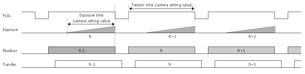
Off : 카메라가 Freerun 모드로 동작합니다. Internal Trigger 신호가 생성되며 그 주기는 Acquisition Frame Rate에 의해 결정됩니다. Acquisition Frame Rate Enable이 Off이면 현재 설정에서 가능한 최대 Frame Rate로 동작합니다.
On : 카메라가 Trigger 모드로 동작합니다. Frame Grabber의 CC1~CC4(Line1~4), GPIO(Line5~6) 또는 Software Trigger를 통해 Trigger를 입력받을 수 있습니다.
Item Setting Value Description Trigger Source Line1, Line2, Line3, Line4, Line5, Line6, Software Trigger 입력으로 사용하고자 하는 Source를 선택합니다. Trigger Delay 0x1 ~ 0xFFFFFFFF Trigger Delay를 조정합니다. (TRGDLY) Line Debounce Time 0x1 ~ 0xFFFF Line Debounce Time을 조정합니다. (TRGFLTNUM)
4.2.2 Trigger Software
Trigger Mode를 ‘On’, Trigger Source를 ‘Software’로 설정하면 적용됩니다. Execute 시 Trigger Pulse를 하나 입력받아 영상 Frame을 한 장 취득할 수 있습니다.
4.2.3 Trigger Source
Camera Link Connector — Line1~4 : CC1~CC4 핀을 통해 Frame Grabber에서 Trigger를 입력받습니다.6pin Connector — Line5 : 2번 핀(GPIO1), Line6 : 3번 핀(GPIO2)을 통해 Trigger를 입력받습니다.Software Trigger — Software 함수를 통해 Trigger를 생성합니다.4.2.4 Trigger Delay
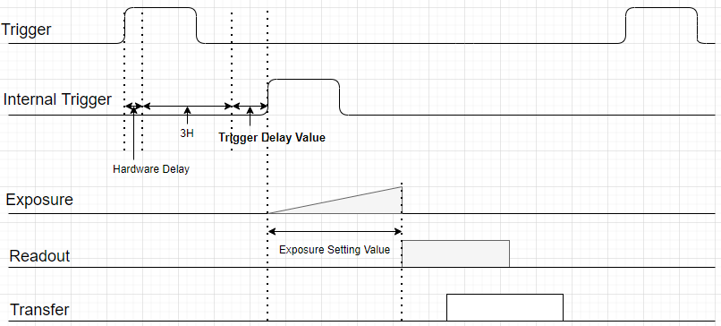
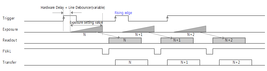
Trigger 입력 후 사용자가 설정한 Delay 시간만큼 지연한 뒤 동작하도록 설정하는 기능입니다. TRGDLY 명령으로 µs 단위 조정이 가능합니다.
Trigger Delay Timing ※ 1H = 74.25MHz(Global Model) 또는 72MHz(Rolling Model) × HMAX (RHMAX 명령어 또는 CamGuideCL에서 확인)
※ Hardware Delay : < 2µs (4.3.1 참고)
4.2.5 Line Debounce Time
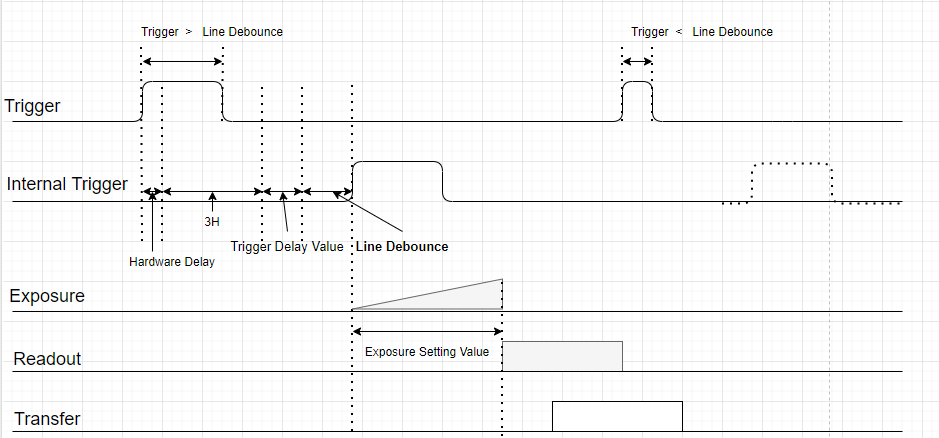
외부 I/O로 전송된 Trigger 신호의 채터링 노이즈를 필터링하는 기능입니다. Line Debounce Time보다 폭이 짧은 Trigger Signal을 노이즈로 간주하여 필터링합니다. TRGFLTNUM 명령으로 µs 단위 조정이 가능합니다.
Line Debounce Timing 4.2.6 Fine Shutter Enable (Unit Control)
Pixel Clock 기준으로 노광 시간을 1µs 단위로 조절하도록 지원하는 기능입니다. ‘On’일 때는 µs 단위, ‘Off’일 때는 HD 단위로 조절합니다.
4.2.7 Exposure Mode
카메라 노광 방식을 결정하는 기능입니다.
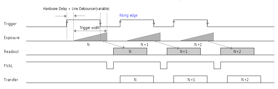
Mode Description Timed 설정되어 있는 시간 값만큼 노광합니다. Trigger Width 입력된 Trigger 신호의 Pulse 폭만큼 노광합니다. Trigger Active가 Rising Edge이면 High인 시간, Falling Edge이면 Low인 시간만큼 노광합니다.
※ Exposure Mode별 Timing
1) Freerun Mode Timing 2) Trigger Timed Mode Timing 3) Trigger Width Mode Timing 4.2.8 Exposure Time
노광 시간을 설정합니다. Timed 모드로 설정되어 있을 때만 적용됩니다. SHTSET 명령으로 µs 단위 조정이 가능합니다. (Range : 0x1 ~ 0xFFFFFFFF)
※ 실제 노광 시간 : 설정 시간 + 14.26µs 또는 13.73µs (2.2 주요 사양 참고)
4.2.9 Exposure Auto
Exposure Time을 자동 조정하여 사용자가 원하는 밝기를 일정하게 유지하는 기능입니다. Exposure Mode가 Timed로 설정되어 있을 때 사용할 수 있습니다.
Item Setting Value Description Exposure Auto Off Exposure Time을 수동으로 설정합니다. Once 한 번만 노광 시간을 조절하여 원하는 밝기 값으로 변경합니다. Continuous 지속적으로 노광 시간을 조절하여 원하는 밝기 값을 유지합니다. Auto Exposure Target 0 ~ 255 사용자가 원하는 밝기 값 설정 (DN, 8bit 기준) Auto Exposure Time Lower Limit 100µs ~ 3sec 자동 설정 가능한 Exposure Time 최소값 (AEMIN). Upper Limit보다 클 수 없습니다. Auto Exposure Time Upper Limit 100µs ~ 3sec 자동 설정 가능한 Exposure Time 최대값 (AEMAX). Lower Limit보다 작을 수 없습니다.
※ Exposure Time 설정 값은 Width/ADC Bit 설정에 따라 달라질 수 있습니다.
4.2.10 Acquisition Frame Rate Enable
Item Setting Value Description Acquisition Frame Rate Enable Off 현재 카메라 설정에서 최대 Frame Rate로 동작합니다. On 설정된 Frame Rate로 동작합니다. Acquisition Frame Rate 1 ~ Max Value Max 값은 모델과 해상도에 따라 달라집니다.
4.3 Digital I/O Control
외부 I/O 신호를 설정할 수 있는 기능입니다.
Item Setting Value Description Line Selector Line1, Line2, Line3, Line4, Line5, Line6, Software 설정을 원하는 Line을 선택합니다. Line Mode Input, Output Line 5, Line 6만 Output으로 설정할 수 있으며 이후 Line Source가 적용됩니다. Line Inverter 0, 1 Enable 시 입력된 신호를 반전시킵니다. Line Status 0, 1 선택된 Line의 현재 상태를 반환합니다. Line Source Off 사용 안 함 Timer1 Active 카메라 내 생성된 파형을 출력합니다. Exposure Active 카메라 노광 시간 동안 활성화됩니다. UserOutput1 / 2 / 3 Input과 별개로 사용자가 설정한 출력값을 유지합니다. User Output Selector 사용할 저장값을 선택합니다. User Output Value 0, 1 User Output Selector에 의해 선택된 값을 설정합니다.
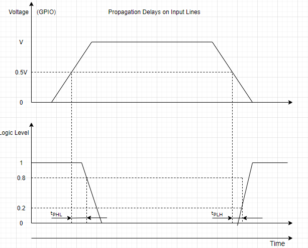
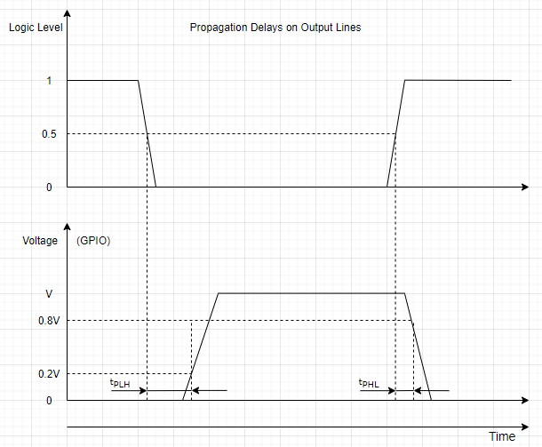
4.3.1 Hardware Propagation Delay (GPI/O)
Rising (tPLH) (<20%) Falling (tPHL) (>80%) Input Line 0.52µs 0.03µs Output Line 1.34µs 0.17µs
Propagation Delays on Input Lines Propagation Delays on Output Lines
4.4 Counter and Timer Control
Strobe 신호 설정 및 영상 출력을 확인하는 기능입니다.
Item Setting Value Description Timer Selector Exposure Exposure : 노광 시작 시점부터 파형 생성 Timer Duration 0 ~ 57,844,677 Strobe 신호의 High 시간을 설정합니다. (FLASHTIME) Timer Delay 0 ~ 57,844,677 Strobe 신호의 Delay 시간을 설정합니다. (FLASHDELAY) Counter Event Source ExternalTriggerStart 외부 Trigger 입력 개수, 노광 시작/종료 횟수, Sensor FVAL 개수 및 비정상 노광 시작/종료 횟수를 선택해 Count합니다. Counter Value 0 ~ 4,294,967,295 Event Source의 Count 값을 표시합니다. Acquisition Start 시 초기화됩니다.
Timer Duration — FLASHTIME 명령으로 µs 단위 조정Timer Delay — FLASHDELAY 명령으로 µs 단위 조정
4.5 Analog Control
4.5.1 Gain Control
Gain을 조정할 수 있는 기능입니다.
Item Setting Value Description Gain Selector All, DigitalAll 설정할 Gain을 선택합니다. Gain Raw All : 0 ~ 240 Gain 값을 수치로 적용합니다. 이미지 신호와 Noise가 함께 증가할 수 있습니다. Gain Abs All : 1 ~ 15.8 Gain 값을 배율로 적용합니다. Gain Auto Off Gain을 수동으로 설정합니다. Once 한 번만 Gain을 조절하여 원하는 밝기로 변경합니다. Continuous 지속적으로 Gain을 조절하여 원하는 밝기를 유지합니다.
Gain Auto와 Auto Exposure를 함께 사용할 경우, 밝아지는 경우 Exposure Control 후 Gain이 적용되고, 어두워지는 경우 Gain Control 후 Exposure가 적용됩니다.
4.5.2 Black Level Control
영상 신호의 DC Offset을 조정하는 기능입니다.
Item Setting Value Description Black Level Selector All, DigitalAll 설정할 Black Level을 선택합니다. Black Level Raw All(ADC 8bit) : 0 ~ 255 아날로그 Black Level을 제어하고 이미지 신호의 DC Offset을 조정합니다.
4.5.3 Gamma Control
Item Setting Value Description Gamma Enable Disable, Enable Gamma 기능 활성화 여부를 결정합니다. Gamma 0 ~ 4.0 Gamma 수치를 조정합니다.
4.5.4 Balance Ratio Control
색 Gain을 맞추기 위한 기능입니다.
Item Setting Value Description Balance Ratio Selector Red, Green, Blue 색 Gain을 조정할 색을 선택합니다. Balance Ratio 0 ~ 4095 선택된 색상에 대해 Gain 수치를 조정합니다. Balance White Auto Off, Once, Continuous Once : 한 번만 White Balance 조정
※ Balance White Auto 사용 시 흰 종이처럼 일정한 밝기의 피사체 조건에서 동작시키면 더 나은 결과를 얻을 수 있습니다.
4.5.5 Noise Reduction
Noise Filter로 영상 Noise를 줄이는 기능입니다. 사용 시 영상의 Edge가 손상될 수 있습니다.
Item Setting Value Description Noise Reduction Enable Disable, Enable Noise Reduction 기능을 활성화합니다.
4.6 LUT Control
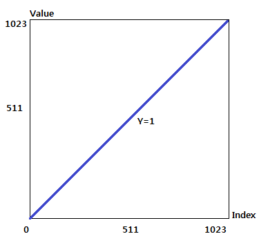
LUT 기능은 영상 신호를 비선형으로 조정하기 위한 기능입니다.
Item Setting Value Description LUT Enable Disable, Enable LUT 기능 활성화 여부를 결정합니다. LUT Index 0 ~ 1023 LUT의 Index 값을 조정합니다. LUT Value 0 ~ 1023 해당 LUT Index의 값을 조정합니다.
LUT Example (V=I) 4.7 Defect Pixel Correction
Defect Pixel을 조정해 주는 기능입니다.
Item Setting Value Description Defect Filter Enable Off, On 보정 값의 활성화 여부를 선택합니다. Defect Filter Test Mode Selector Off, Mark Black, Mark White, Mark White with Black Background 보정 위치를 검게, 밝게, 또는 검은 배경 위 밝게 표시합니다. Defect Pixel Replacement Count 1 ~ 512 최대 보정할 Defect Pixel 개수를 지정합니다. Defect Pixel Index 0 ~ 511 보정할 Defect Pixel Index를 선택합니다. Defect Pixel X Coordinate 0 ~ WidthMax-1 보정할 Pixel의 X축 좌표를 입력합니다. Defect Pixel Y Coordinate 0 ~ HeightMax-1 보정할 Pixel의 Y축 좌표를 입력합니다. Defect Pixel Replace Execute Execute 입력된 보정값을 정렬 후 적용합니다.
4.8 Flat Field Correction
촬상한 이미지의 밝기 값을 균일하게 보정하는 기능입니다.
Item Setting Value Description FFC Enable Off, On 보정 값의 활성화 여부를 선택합니다. Black Calibration Execute 어두운 이미지를 통해 FPN을 보정합니다. White Calibration Execute 밝은 이미지를 통해 PRNU를 보정합니다. FFC Save Load Flash Select 0 ~ 3 FFC 데이터를 읽고 저장할 영역을 선택합니다. FFC Save Execute 선택된 영역에 FFC 데이터를 저장합니다. FFC Load Execute 선택된 영역의 FFC 데이터를 읽어옵니다.
4.9 User Set Control
사용자가 설정한 값을 저장하거나 불러오기 위한 기능입니다.
Item Setting Value Description User Set Selector Default, UserSet1, UserSet2, UserSet3 Default는 출하 설정으로 Load만 가능합니다. UserSet1/2/3은 사용자가 Save/Load할 수 있으며 전원 Off/On 시에도 유지됩니다. User Set Load Execute 선택된 User Set 설정을 불러옵니다. User Set Save Execute 선택된 User Set 영역에 설정을 저장합니다.
5. 카메라 외관
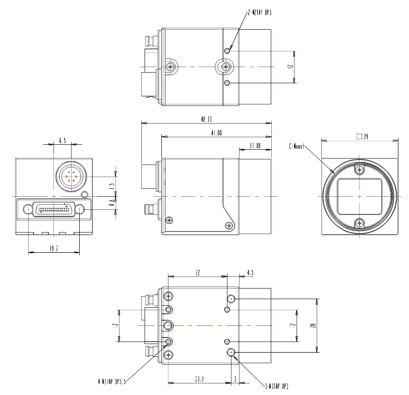
SMCL1 Series Camera Dimensions
6. UART 통신
6.1 Communication Setting
Item Setting Value Baud Rate Default 9,600bps Data Bit 8bit Parity None Stop Bit 1bit Flow Control None
W or Rnote1 Command Space Valuenote2 Enter
※ note1 : W — Write, R — Read
6.3 Register Area
Area Read Write Factory Area O X (Only factory write) User 1 Area O O User 2 Area O O User 3 Area O O
6.3.1 Register SAVE
Command Index Description SAVE 1 ~ 3 User Area Register Save
6.3.2 Register LOAD
Command Index Description LOAD 0 Factory Area Register Load LOAD 1 ~ 3 User Area Register Load
6.4 Register List
CamGuide_CL software 및 Appendix A를 참조하십시오.
Appendix A. UART Command List
Group R/W Command Parameter Description
System Control - SAVE 0:Factory, 1~3:User Save to EEPROM - LOAD 0:Factory, 1~3:User Load from EEPROM R/W UID 0:Factory, 1~3:User User ID R SN String Read Serial Number W BAUDRATE 0x2580:9600 / 0x4B00:19200 / 0x9600:38400 / 0xE100:57600 / 0x1C200:115200 / 0x38400:230400 Baud Rate Write R EEPIDX 0:Factory, 1~3:User Read Selected EEPROM Index R MODEL String Read Camera Model Name R VER String Firmware Version R XMLFILE String Read XML File Version R TEMP [15:0] Data Read Temperature Value Acquisition Control R/W FREERUN [31:0] Data Run-Free Time (µs) R/W SHTSET [31:0] Data Shutter (µs) R/W FREERUNEN 0:Disable, 1:Enable Freerun Time User Control Enable R MINFREERUN [31:0] Data Read Min Freerun Time (µs) R MINSHTSET [31:0] Data Read Min Exposure Time (µs) R REALFREERUN [31:0] Data Real Freerun Time (µs) R/W AEMAX [31:0] Data Auto Exposure Max Time (µs) R/W AEMIN [31:0] Data Auto Exposure Min Time (µs) R/W AECMODE 0:Off, 1:Once, 2:Continuous Auto Exposure Control Mode R/W AETARGET 0 ~ 255 Auto Exposure Target Value R/W TRGMODE 0:Disable, 1:Enable Trigger Mode Enable R/W EXPMODE 0:Timed, 1:Pulse Width Control Exposure Mode R/W TRGSRC 0:CC1, 1:CC2, 2:CC3, 3:CC4, 4:GPIO1, 5:GPIO2, 7:Software Select Trigger Source Pin R/W TRGDLY [31:0] Data Trigger Delay (µs) R/W TRGFLTNUM [31:0] Data Trigger Filter Number (µs) W SWTRIG - Software Trigger Event Assert R/W HSTMODEEN 0:Disable(HD), 1:Enable(µs) Unit Control Enable R/W TAPCFG 1:1Tap, 2:2Tap, 3:3Tap Number of CameraLink Output Taps Image Format Control R/W PIXFMT Mono: 0x01080001 Mono8, 0x01100003 Mono10 Pixel Format Select R/W ADCBIT 8, 10, 12bit Sensor AD Conversion Bits Setting R PIXCLK [31:0] Data Read Pixel Clock (Hz) R STMCLK [31:0] Data Read Stream Clock (Hz) R HMAX [31:0] Data Read 1HD Size R/W ISCOLOR 0:Disable, 1:Enable Color Mode Enable R BAYERORD 0:RG, 1:GR, 2:GB, 3:BG Read Bayer Order R/W OUTSEL 0:Off, 1:Horizontal, 2:Vertical, 3:Horizontal+Vertical Select Test Pattern R/W FLIPMODE 0:Normal, 1:Y, 2:X, 3:X&Y Flip Mode Select R/W BEN [1:0] Data (11, 12, 21, 22) Image Mode Binning R/W SKIP [1:0] Data (11, 12, 21, 22) Image Mode Decimation R/W WIDTH 8bit: 520~WidthMax / 10·12bit: 264~WidthMax Image Width Size Control R/W HEIGHT 4 ~ HeightMax Image Height Size Control R/W OFFSETX 8bit: 0~WidthMax-520 / 10·12bit: 0~WidthMax-264 Image Offset X Control R/W OFFSETY 0 ~ HeightMax-4 Image Offset Y Control R WIDTHMAX [31:0] Data Read Image WidthMax Size R HEIGHTMAX [31:0] Data Read Image HeightMax Size R/W SHTMODE 0:Rolling, 1:Global Reset Shutter Mode Select FFC Control R/W FFCEN 0:Disable, 1:Enable Flat Field Correction Enable W FFCSAVE - Flat Field Correction Data Save W FFCLOAD - Flat Field Correction Data Load W BLACKCAL - FPN Correction W WHITECAL - PRNU Correction LUT Control R/W LUTEN 0:Disable, 1:Enable Look Up Table Enable R/W LUTDATA X:0~1023, Y:0~1023 Look Up Table Data (10bit to 10bit) R/W GAMMAEN 0:Disable, 1:Enable Gamma Enable R/W GAMMA Gamma Data × 65536 Gamma Data Defect Pixel Correction R/W DEFCOREN 0:Disable, 1:Enable Pixel Defect Correction Enable R/W DEFHIGHLIGHT 0:Normal, 1:Mark Black, 2:Mark White, 3:Mark White with Black Background Defect Correction Test Mode Select R/W DEFCNT 1 ~ 512 Defect Correction Write Count W IMMDEFCOR - Immediate Defect Correction Execution W DEFEXEC - Defect Correction Execution Trigger / Counter Control R/W FLASHSRC 0:Exposure Start, 1:Trigger Start, 2:Internal VD Flash Time Reset Signal Select R/W FLASHDELAY [31:0] Data Flash Delay (µs) R/W FLASHTIME [31:0] Data Trigger Time (µs) R TRGSTARTCNT [31:0] Data Read External Trigger Count R EXPSTARTCNT [31:0] Data Read Exposure Start Count R EXPENDCNT [31:0] Data Read Exposure End Count R FRAMEENDCNT [31:0] Data Read Sensor FVAL Receive Count R EXPSTARTMISSCNT [31:0] Data Read Exposure Start Error Count R EXPENDMISSCNT [31:0] Data Read Exposure End Error Count Digital I/O Control R/W LINEMODE 4:GPIO1, 5:GPIO2 / 0:Input, 1:Output Line Mode Select R/W LINEINVEN 0:CC1, 1:CC2, 2:CC3, 3:CC4, 4:GPIO1, 5:GPIO2 / 0:Disable, 1:Enable Line Inverter Enable R/W LINESRC GPIO1/2 : Timer, Exposure, UserOutput1~3, Off Line Source Select R LINESTATUS bit[x]:Line Number Read GPIO Status R/W USEROUTPUT 0:User1, 1:User2, 2:User3 / 0:Disable, 1:Enable GPO User Output Value Analog Control R/W GAIN Range: Model dependent Master Sensor Gain R/W DGAIN [12:10] Decimal, [9:0] Fractional Digital Gain R/W CLAMP 8bit:0~255 / 10bit:0~1023 / 12bit:0~4095 Master Sensor Clamp R/W DCLAMP 0 ~ 1023 Digital Clamp R/W AGCMODE 0:Off, 1:Once, 2:Continuous Auto Gain Control Mode R/W AWBMODE 0:Off, 1:Once, 2:Continuous Auto White Balance Mode R/W RGAIN [12:10] Decimal, [9:0] Fractional Red Gain R/W GGAIN [12:10] Decimal, [9:0] Fractional Green Gain R/W BGAIN [12:10] Decimal, [9:0] Fractional Blue Gain R/W NREN 0:Disable, 1:Enable Hybrid Filter Enable
Appendix A Notes
Note 1 — Model별 ADC / Binning / Decimation 지원
Model ADC Bit Binning Decimation H V H+V H V H+V MC-A160M 8,10,12 X O O O O O MC-A160K 8,10,12 X X X O O O MC-A040M/K 8,10,12 X X X X X X MC-A500M/K 12 X X X O O O MC-A320M/K 12 X X X O O O MC-A121M/K 12 X X X O O O MC-A121R/L 10 X X X X X X
※ H : Horizontal, V : Vertical, H+V : Horizontal Vertical
Note 2 — MC-A121R(L) Clamp Range 0 ~ 255
Note 3 — 카메라별 최소 HMAX 값
Model Pixel Clock HMAX(min) 1H(min) MC-A040x-523 74.25MHz 238 Clock 3.20µs MC-A160x-154 74.25MHz 242 Clock 3.25µs MC-A320x-55 74.25MHz 846 Clock 11.39µs MC-A500x-35 74.25MHz 996 Clock 13.41µs MC-A500M-LF 74.25MHz 996 Clock 13.41µs MC-A121x-20 74.25MHz 1041 Clock 14.02µs MC-A121R(L)-20 72.00MHz 865 Clock 12.01µs
※ 1H = 74.25MHz(Global Model) 또는 72MHz(Rolling Model) × HMAX (RHMAX 명령어 또는 CamGuideCL에서 확인)
Appendix B. 카메라 동작 준비
1. SDK 설치
CamGuideCL_V2.3.4_x64.exe : Windows 64bit용 설치 프로그램
※ 버전은 향후 업데이트될 수 있습니다.
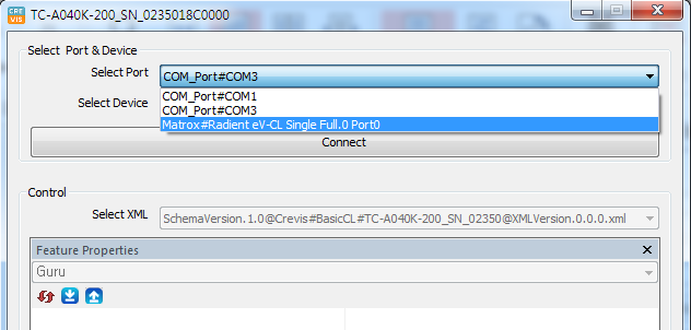
2. 카메라 통신 연결 방법
2.1 CamGuideCL 실행
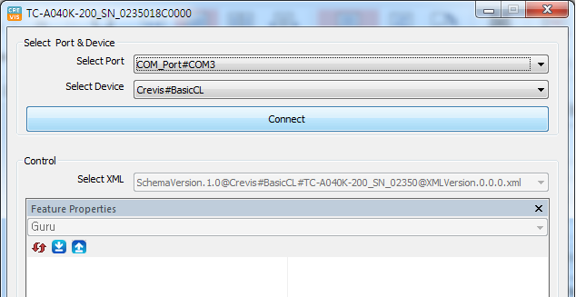
2.2 Select Port : 카메라가 연결된 포트 선택
Select Port 2.3 Connect 클릭
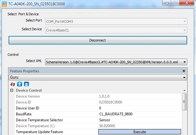
Connect 2.4 연결 완료
연결 완료 ※ 상세 설명은 CamGuideCL 매뉴얼을 참조하십시오.
Revision History
Revision Date Changes Remark 1.0 2019.04 Issued 1.1 2020.02 목차 수정 및 Fine Shutter 설명 추가 1.2 2020.08 Appendix A 수정 1.3 2020.09 Trigger Delay, Line Debounce 항목 개선